From Breadboard Prototype to Working PCB
After iterating on breadboard prototypes for a low-power e-paper thermometer, I was curious to see if I could turn them into a working single PCB design. In this post I explore how I used Claude Code to help with the prototype-to-PCB transcription, and where it fell short.
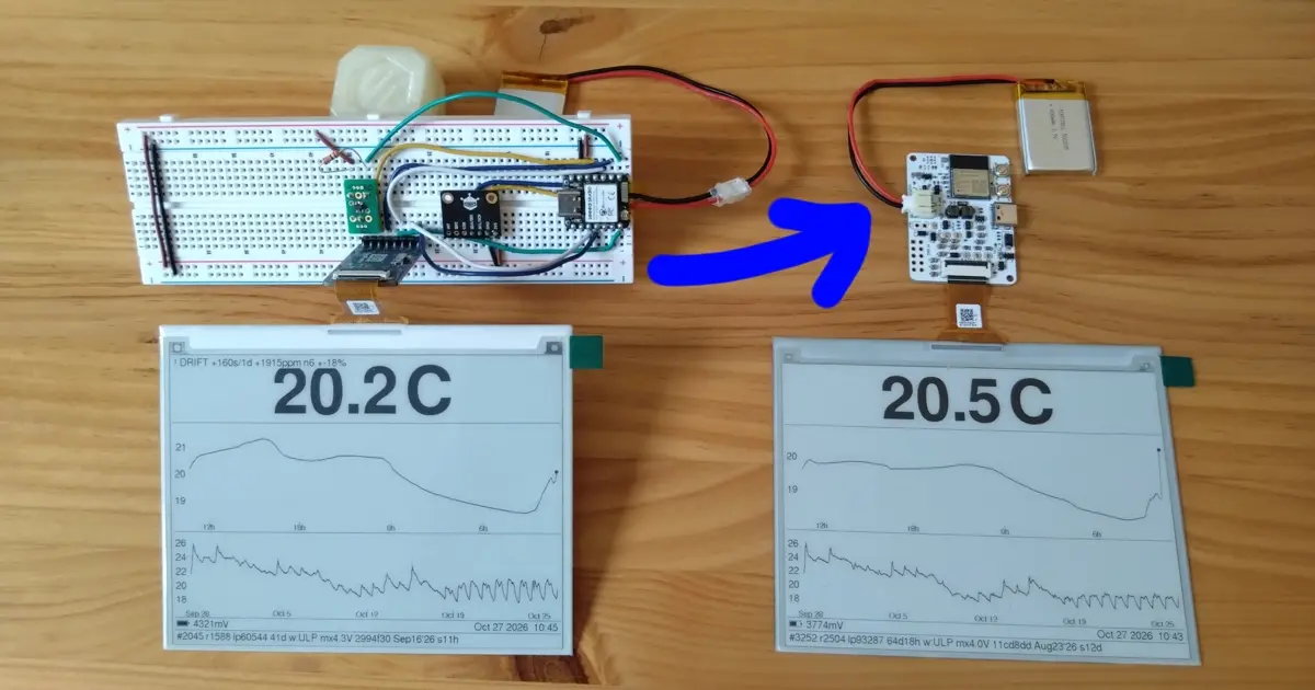
How it started
I’ve always been fascinated with e-ink displays and their ability to keep an image with zero power consumption. Back in 2021 I started building a small battery-powered ESP32-based thermometer to explore those characteristics. It was kind of bulky. Its temperature polling also didn’t leverage the ESP32’s ultra-low-power (ULP) core, so polling ended up dwarfing the display’s power budget.
Earlier this year, I gave it a second go with Claude Code’s help, which successfully implemented bit-banged I2C polling of the BMP390L sensor using assembly for the ESP32-WROOM’s ULP core. I then explored what things would look like on a more recent ESP32-C6, which supports C programming of its LP cores, and managed to get power consumption down low enough that a single 400 mAh battery now theoretically lasts more than a year1.
While the prototypes worked fine, they were a spaghetti mess of wires and various components on a breadboard - collecting dust, fragile when moved, and overall not looking great. Given low-cost manufacturing options from PCBWay and JLCPCB, I was curious to see if I could leverage Claude Code2 to help me get to a functional design.
The objective
My primary objective was to get to a board with the following characteristics:
- Ultra-low power usage - integrating learnings from the various prototype builds;
- Small footprint - ideally no larger than a 1.54" e-paper display;
- USB-C connectivity for firmware updates and charging;
- FPC connectivity for Good Display e-paper displays;
- JST-2 battery connector;
- Reasonable cost;
- Open-source KiCad PCB design.
Schematic
In prototype form, components typically included:
- An ESP32 development board with low deep-sleep power consumption, such as the Seeed Studio XIAO ESP32-C6 or the Firebeetle ESP32-E. These provide Wi-Fi, USB connectivity, battery charging, SPI needed for the e-paper display, I2C for the temperature sensor, ADC for battery voltage sensing, and numerous GPIO pins, as well as a couple of hardware buttons and LEDs.
- A temperature sensor such as Bosch’s BMP581 or BMP390L with very low deep-standby consumption.
- An adapter like Good Display’s DESPI-C02 to connect the ESP32 to an e-paper display.
- A MOSFET to prevent the display adapter from consuming power when not active.
- A couple of resistors acting as a voltage divider to measure battery voltage on one of the ESP32’s ADC pins.
Electronic component manufacturers are very good at publishing detailed datasheets which, in conjunction with the prototype wiring diagrams, made for a great starting point.
Requirements were inferred from component datasheets, prototype wiring information and experimental results. Noteworthy changes from the prototypes included:
- Using an LDO regulator for voltage conversion because the XIAO ESP32-C6’s buck converter caused brownouts below 3.7V.
- Selectable resistor and inductor values for the EPD booster stage to match various panel requirements.
- A clock crystal to fix clock drift observed on deep-sleeping ESP32s.
Claude wrote a circuit generator to hold the logical schematic of components and the connecting electrical nets. Sub-agents role-playing experienced low-power electronics design engineers were used as reviewers. The generator output a KiCad .kicad_sch file, which could also be used to run through KiCad’s electrical rules checker (ERC). This gave additional confidence that the circuit didn’t have any common issues such as unconnected or incorrectly connected pins. This step was uneventful.
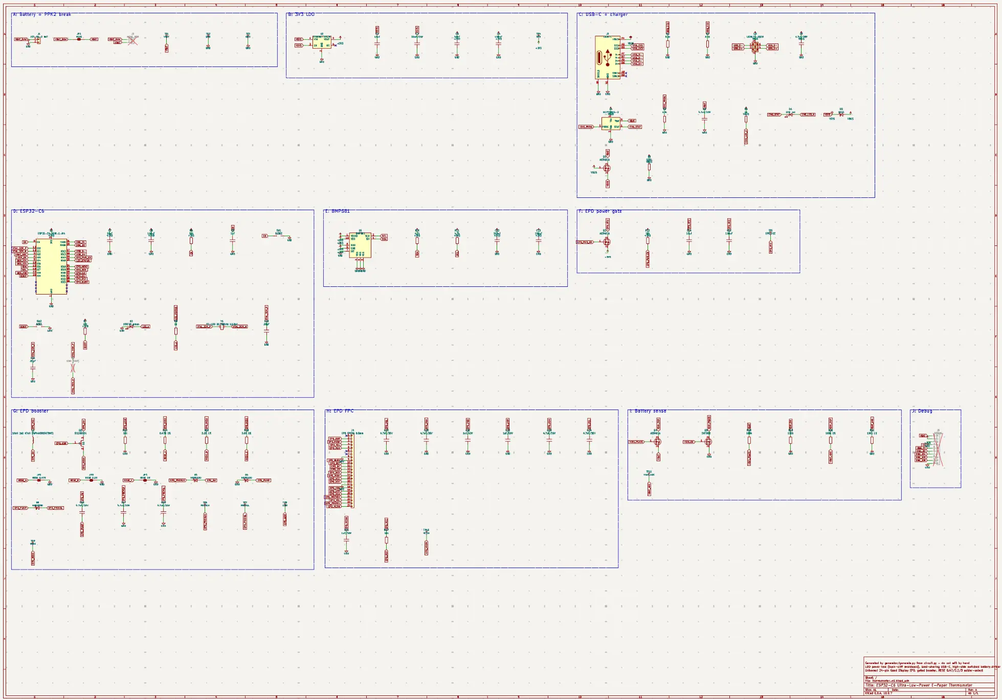
Where Claude struggled a bit more was producing a human-readable version of the schematic’s layout. While it was logically sound, it looked nothing like something a human would have produced, showing disconnected individual components rather than connected functional zones. It also didn’t account for legibility of the schematic, with unnecessary wire crossings and overlapping labels. The solution ended up being an agent-placed layout of each component on the schematic with a generator computing wire routing and label placement to optimize for clarity3.
| Initial schematic | Final schematic |
|---|---|
 | 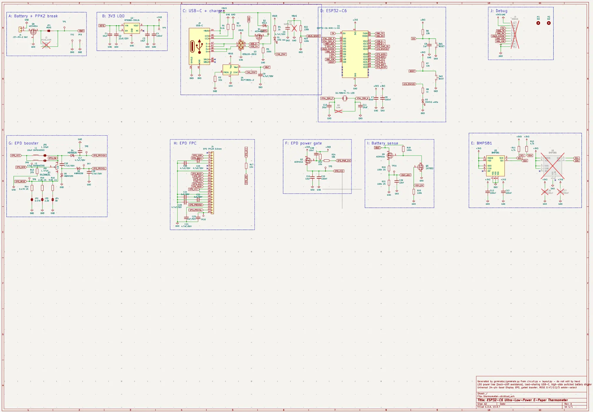 |
With this legible schematic in hand, I was able to manually cross-check the different subcircuits against the reference schematics published for the prototype boards. Reassuringly, this didn’t turn up any issues.
Placement & routing
Going from a schematic to a manufacturable PCB involves physically placing components on the board, and routing copper traces to connect them as per the schematic. This is a hard problem to automate. Claude Code failed to work it out. It was somewhat decent at placing components on the board, and designing silkscreen markings to match. But after 5 days of working on the problem, it still had not routed 9 of the most complex nets and the entire ground net4.
Up to that point all KiCad files had been entirely programmatically generated through agent-authored Python. Successfully routing, and optimizing placement, required me to get directly involved. I switched to the following hand-routing loop to iterate through the problem:
[agent]Make a working copy of the.kicad_pcbfile for me to work on;[human]Route nets, place vias, set trace widths, move components, update silkscreen in the KiCad UI;[agent]Harvest changes back into the generator;[agent]Verify all gates still pass, including KiCad’s design rules checker (DRC);[agent]Commit.
As classes of DRC problems were fixed, Claude was able to verify compliance and refine rules5 while I solved outstanding errors.
| Agent placement & routing | Human placement & routing |
|---|---|
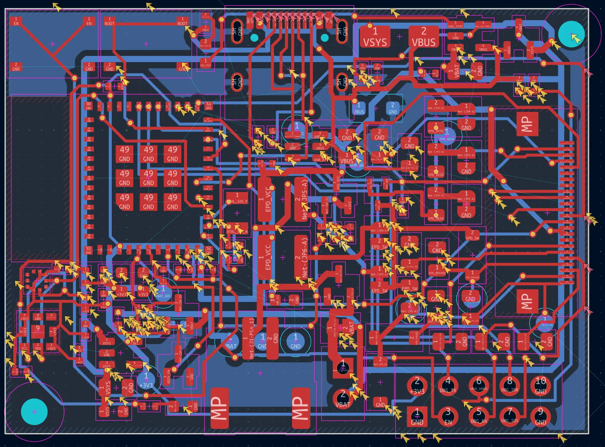 | 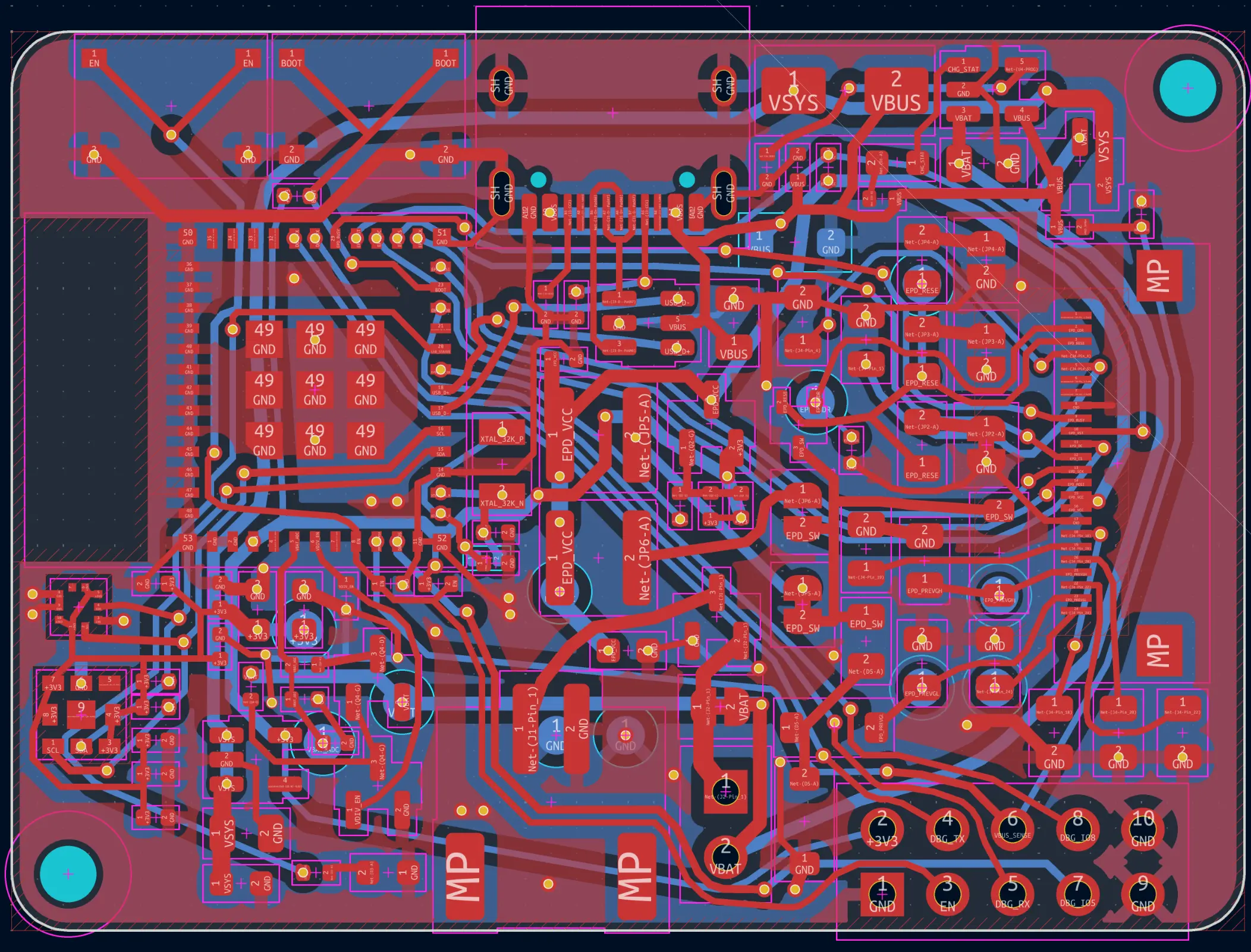 |
Claude’s lack of geometric intuition meant it couldn’t effectively reason through the problem6. Because the PCB placement & routing problem is much harder than the schematic layout one, its typical algorithmic approach was not successful. I, on the other hand, found it far more tractable. It was similar to iteratively solving a set of geometrical puzzles, which the human brain is very good at.
Ordering … and where Claude fell short
After 7 days of iterating on the PCB, I was finally confident enough to start looking at ordering the board for manufacturing with JLCPCB. I’d never used their services before. They are most amazing! I’ll spare you the details - the full order setup is documented if you’re interested.
I was worried when ordering that the generated Gerber files - used as input to the manufacturing process - would have errors that would only show up on the physical board. For example, a part’s 3D representation and its footprint could be improperly modeled in KiCad, resulting in components being installed in the wrong location. Somewhere along the way, JLCPCB offered a 3D render of the board with a note that 3D model placement might still be inexact. I had confirmed with their support that a technician would properly verify and adjust.
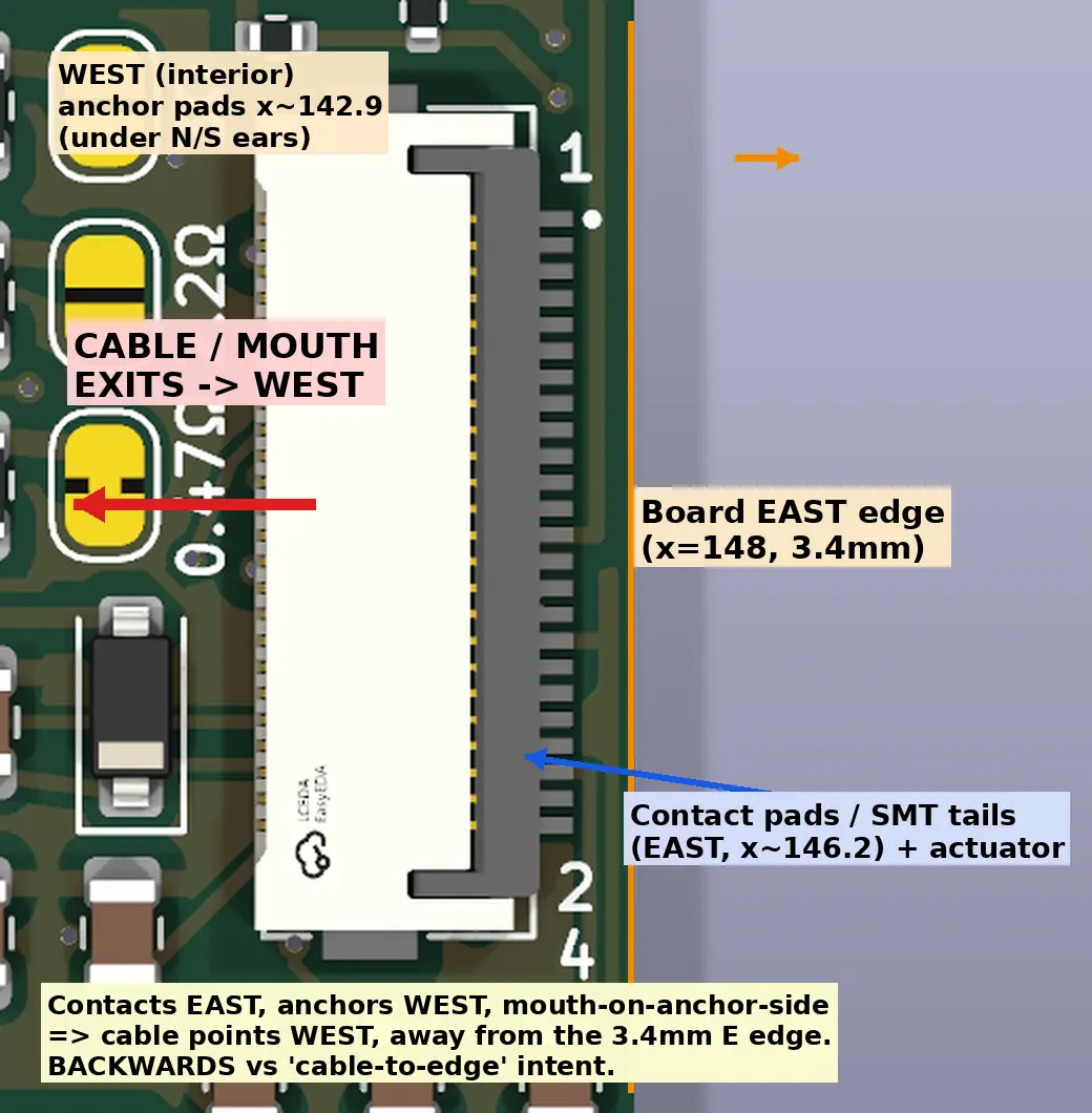
What they wouldn’t catch, though, was the e-paper FPC connector and the USB-C connector both being improperly modeled. Inspecting their render, I noticed the FPC connector was mounted backwards, and that the USB-C connector, while correctly oriented, had an inverted footprint.
Here is a view of the FPC connector from JLCPCB’s render. The soldered pads, which sit opposite the connector’s mouth, are on the PCB’s outside edge instead of facing inward:
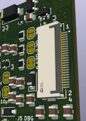
As with the USB connector, the FPC connector was not available in KiCad’s footprint library, so Claude read the datasheet to model its own. What was interesting here was not that it got it backwards (that happens), but that it persisted in telling me it was right several times in a row despite obvious evidence to the contrary. The key to fixing its flawed reasoning was to instruct it to produce annotated proofs on top of the datasheet drawings and KiCad 3D renders.
| Section | Land Pattern | Board |
|---|---|---|
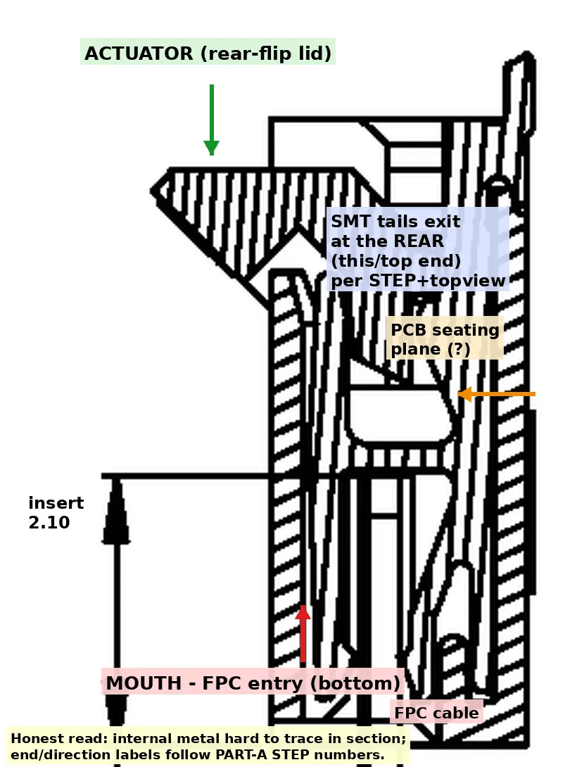 | 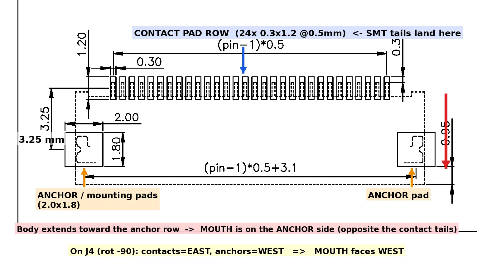 |  |
For a task like this, which cannot be proven correct programmatically, I find it interesting that showing your work, as you would with a colleague, works. Rather than reasoning over words, the key here was to ask it to tie its results back to the original data it was reasoning from - in this case engineering drawings and 3D renders. See proving a part’s geometry for more details. To generalize, tying claims back to their original sources helps ensure correctness.
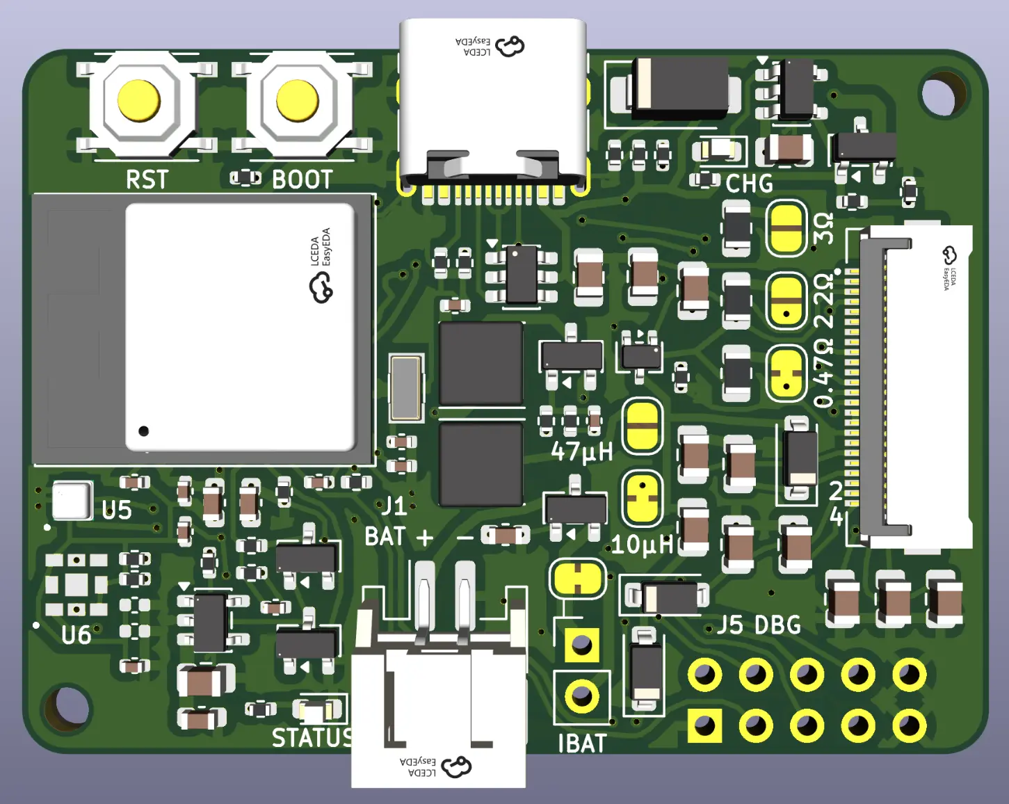
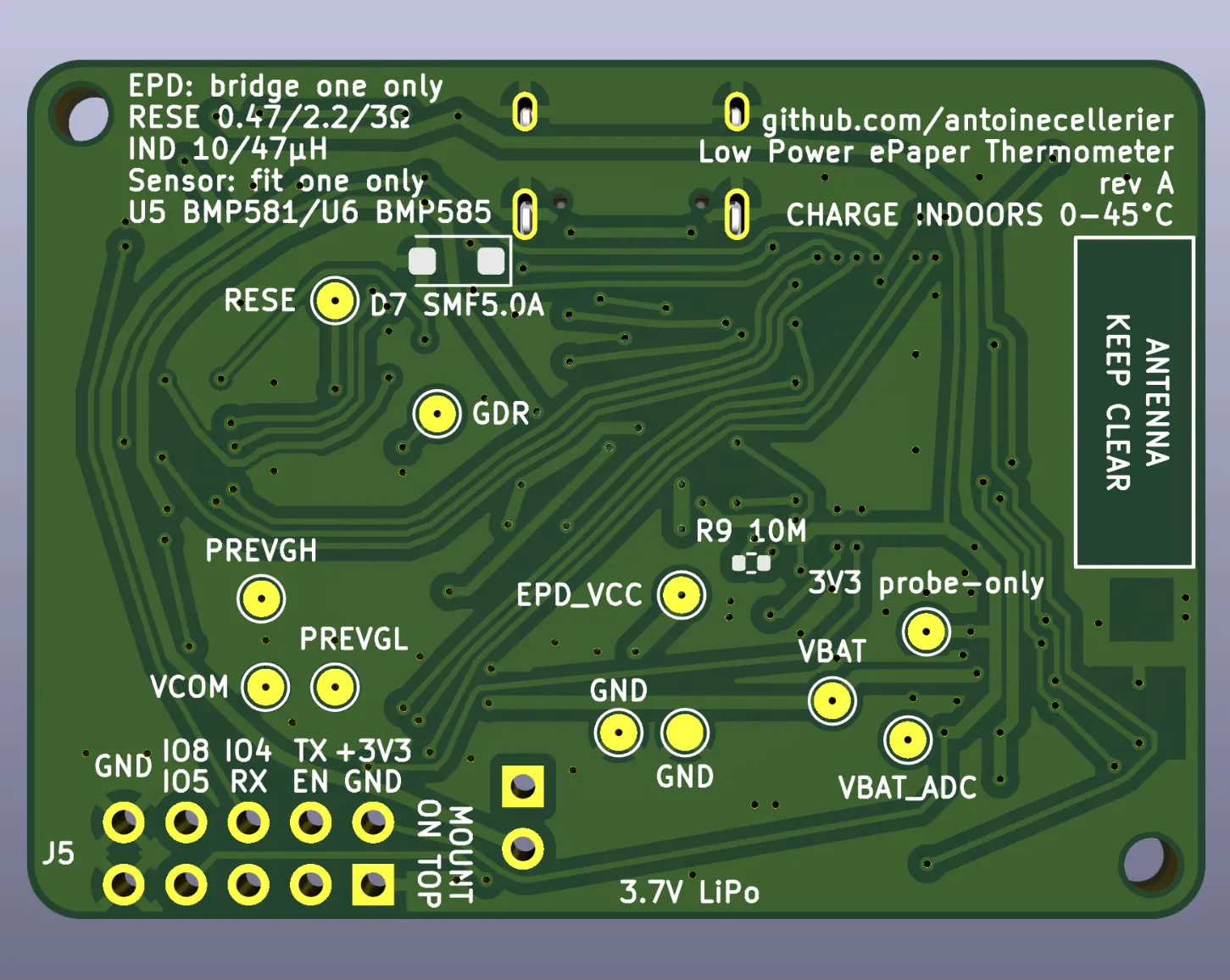
Of course flipping the FPC and USB-C connectors meant most of the routing, some of the placement, and the silkscreen had to be redone - yay! It actually ended up being a good thing, as the resulting topology was simpler.
| PCB front | PCB back |
|---|---|
 |  |
Results and what’s next
Overall this project took two weeks from start to order placement, without any prior experience designing a PCB. I find it impressive that with a bit of critical thinking (and a lot of time stuck indoors because of a heatwave), coding-agent-aided design is able to produce such results.
The boards arrived 9 days later, and everything worked first try. The order added up to ~200€ for 4 fully populated boards and one bare PCB.
There are a few things which could nonetheless be improved for a future version:
- USB power heats up the board, which makes the temperature sensor unreliable when debugging over USB or charging. An experienced electrical engineer would have thought to include proper thermal isolation slots or other mitigations.
- Selectable resistors and inductors ended up not being necessary after real-life testing. Removing them could reduce the number of components on board and simplify routing.
- Some early design decisions, such as via-in-pad (filled and plated over), which added 44€ pre-tax, pushed the price up. A future version could optimize for cost more. Also getting the order under 150€ would avoid needing to pay VAT & associated DHL fees.
Maybe I’ll take things a bit further on the next project, with a foray into robotics?
If you’re also exploring AI-aided physical world interactions, do reach out - I’d love to talk.
Learn more and find instructions to build your own at https://github.com/antoinecellerier/lowpower-epaper-thermometer .
Measurements show a 15 to 20 µA sleep floor and a screen update cycle taking anywhere from 3 to 10 µAh depending on the e-paper display. If you’re curious, a lot of power consumption figures and experiments are recorded at https://github.com/antoinecellerier/lowpower-epaper-thermometer#power-consumption . ↩︎
This was back in July. Models used were Fable 5 and Opus 4.8. ↩︎
It’s still not perfect but was good enough for what I needed. ↩︎
If you know of a potential solution to this, please get in touch! ↩︎
Andrew Klofas’ kicad-happy design review project proved to be another valuable review layer, producing detailed findings. ↩︎
Yes, I’m anthropomorphizing here. ↩︎